LaRA EED - Research Facility Overview
The Laboratory for Radiation and Aging Effects in Electronic Devices (LaRA EED) is hosted by the Department of Elementary Particle Physics (DFPE) of the Horia Hulubei National Institute for R&D in Physics and Nuclear Engineering (IFIN-HH). In this laboratory embedded systems and experimental benches are developed and implemented in order to support high energy physics experiments at particle accelerators and cosmic space applications. Research interest is mainly focused on radiation hardness qualifications of sensors and complex integrated circuits. The reliability of the electronic devices in harsh radiation environment is investigated during tests in particle beams at various external facilities. For end-applications with specific radiation background the behaviour is extrapolated based on data registered before, during and after irradiation. The research infrastructure in the laboratory, consisting of hardware and software tools, and measurement and control instrumentation, allows the personnel to fully design and implement experimental benches for radiation hardness assessment and thus enrich the experience in well defining monitoring strategies to be applied to the devices under test. Recent solid experience was gained by evaluating Application-Specific Integrated Circuits (ASICs) and Field-Programmable Gate Array (FPGA) technologies from the perspective of mixt-field radiation environment encountered in Large Hadron Collider (LHC) experiments. Further expertise was obtained in testing and qualifying optical sensors for single-photon counting. For example, we used a custom locally built light-tight enclosure with associated electronics for the multi-anode photomultipliers (MaPMT) performance evaluation and aging studies - more details details available here.
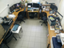
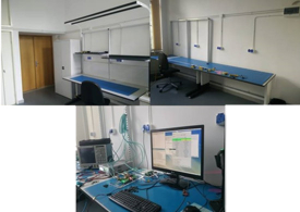
LaRA EED has a space dedicated to PCB design and micro-assembling (left-hand side picture below) and another one for long-term testing under ESD conditions (see right-hand side photos below).


Here is a tentative summary of the test and measurement instruments available at the laboratory: CNC machine for double sided PCB milling; soldering and desoldering stations for THT, SMD, LGA, BGA device packages; high-speed waveform generator; high-performance digital oscilloscopes; bench multimeter and power supplies, handheld digital instruments, logic analyser and FPGA development boards. There is also a full range of software tools for PCB design, circuit simulation, FPGA firmware development, graphical user interface development, data analysis and interpretation.
Deliverables obtained using the research infrastructure
Journal papers
- V.M. Placinta, L.N. Cojocariu and C. Ravariu, Proton-induced radiation effects in the I/O blocks of an SRAM-based FPGA, accepted for publication in Journal of Instrumentation (JINST), September 2019
- L.N. Cojocariu and V.M. Placinta, Ion Beam Irradiation Effects in KINTEX-7 FPGA Resources, Rom. J. Phys. 64 (2019) 901 (link).
- F. Maciuc, L.N. Cojocariu and V.M. Placinta, RICH Upgrade PDMDB-PRR Summary of KINTEX-7 FPGA Testing in Radiation Environments, Extrapolation and Conclusions, in CERN LHCb-RICH Production Readiness Review (PRR) meeting, June 2018.
- V.M. Placinta, L.N. Cojocariu and C. Ravariu, Test Bench Design for Radiation Tolerance of Two ASICs, Romanian Journal of Physics 62, 903 (2017) (PDF)
- L.N. Cojocariu, V.M. Placinta, and L. Dumitru, Monitoring System for Testing the Radiation Hardness of a KINTEX-7 FPGA, in proceedings of the 9th International Physics Conference of Balkan Physical Union, Istanbul University, Istanbul, Turkey, 24–27 August 2015, AIP Conf. Proc. 1722 (2016) 140009. (link)
Conference Talks and Posters
- L.N. Cojocariu, V.M. Placinta, Proton-Induced Radiation Effects in MAROC3, a full readout 0.35 µm SiGe ASIC, Topical Workshop on Electronics for Particle Physics 2019 (TWEPP2019), Santiago de Compostela University, Santiago de Compostela, Spain, September 2nd–6th 2019 (poster)
- V.M. Placinta, L.N. Cojocariu, et al, Radiation Hardness Tests Done on KINTEX-7 FPGA for High Energy Physics Experiments, Topical Workshop on Electronics for Particle Physics 2019 (TWEPP 2019), Santiago de Compostela University, Santiago de Compostela, Spain, September 2nd–6th 2019 (poster)
- L.N. Cojocariu, V.M. Placinta, Investigation of submicron Si-Ge BiCMOS technology node behaviour for two ASIC under proton beam irradiation, The 19th International Balkan Workshop on Applied Physics (IBWAP), July 16th-19th, 2019, Ovidius University of Constanta, Romania, IBWAP Book of abstracts, pp. 113 (abstract & poster)
- V.M. Placinta, L.N. Cojocariu, Radiation hardness assurance of Field Programmable Gate Arrays in LHC experiments, The 19th International Balkan Workshop on Applied Physics (IBWAP), July 16th-19th, 2019, Ovidius University of Constanta, Romania, IBWAP Book of abstracts, p. 128 (abstract & poster)
- V.M. Placinta, L.N. Cojocariu and C. Ravariu, I/O Blocks Reliability for an SRAM Based FPGA when Exposed to Ionizing Radiation, 41th International Semiconductor–Conference CAS2018, October 10th–14th 2018, Sinaia, ROMANIA; (presentation+proceeding)
- V.M. Placinta, L.N. Cojocariu and F. Maciuc, Investigations of Proton Induced Radiation Effects in 0.15 µm CMOS Antifuse FPGA, Topical Workshopon Electronics for Particle Physics (TWEPP2018), September 17th –21st 2018, KULeuven, Antwerp, Belgium (presentation)
- V.M. Placinta, L.N. Cojocariu, Radiation Hardness of Field Programmable Gate Arrays in LHC Experiments, Third Barcelona Techno Week – Course on semiconductor detectors, Barcelona, Spain, July 2017 (poster)
- V.M. Placinta, L.N. Cojocariu and C. Ravariu, Evaluating the Switching Mode Power Supplies Used in Radiation Hardness Tests of Integrated Circuits, 40th International Semiconductor Conference (CAS2017), Sinaia, Romania, October 2017 (presentation+proceeding)
- V.M. Placinta and L.N. Cojocariu, Radiation Hardness Studies and Evaluation of SRAM-Based FPGAs for High Energy Physics Experiments, Topical Workshop on Electronics for Particle Physics 2017, Santa Cruz Institute of Particle Physics (SCIPP), California, USA, September 11th–14th 2017, available at: TWEPP2017 (presentation & proceeding)
- V.M. Placinta, First Results on KINTEX-7 FPGA testing in mixed field radiation at CHARM facility, Topical Workshop on Electronicsfor Particle Physics 2017, Santa Cruz Institute of Particle Physics (SCIPP), California, USA, September 11th–14th 2017, available at: TWEPP2017 (presentation)
- V.M. Placinta, L.N. Cojocariu, et al, Kintex-7 Irradiation, Test Bench and Results, Topical Workshop on Electronics for Particle Physics 2016, Karlsruhe Institute of Technology (KIT), Karlsruhe, Germany, September 26th–30th 2016, available at: TWEPP2016 (presentation)
- L.N. Cojocariu, V.M. Placinta, Designing and implementing test benches for radiation hardness qualifications of readout electronics from LHCb RICH photodetectors, The 15th International Balkan Workshop on Applied Physics (IBWAP), July 2-4, 2015, Ovidius University of Constanta, Romania, IBWAP Book of abstracts, pp. 103-104 (presentation)
- V.M. Placinta, L.N. Cojocariu, Practical test bench used for testing Photomultiplier Tubes, type MaPMT, The 15th International Balkan Workshop on Applied Physics (IBWAP), July 2-4, 2015, Ovidius University of Constanta, Romania, IBWAP Book of abstracts, p. 115 (abstract & poster)


